Cmos Inverter 3D / CMOS Layout Design: Introduction |VLSI Concepts / You might be wondering what happens in the middle, transition area of the.
Dapatkan link
Facebook
X
Pinterest
Email
Aplikasi Lainnya
Cmos Inverter 3D / CMOS Layout Design: Introduction |VLSI Concepts / You might be wondering what happens in the middle, transition area of the.. The two transmission gates work in tandem. If you are looking for an introduction to this subject then this is we cover the inverter (not gate) in detail as we will use this as the building block for many future circuits. Cmos devices have a high input impedance, high gain, and high bandwidth. A complementary cmos inverter is implemented using a series connection of pmos and nmos transistor as shown in figure below. These characteristics are similar to ideal amplifier characteristics and, hence, a cmos buffer or inverter can be used in an oscillator circuit in conjunction with other passive components.
Cmos devices have a high input impedance, high gain, and high bandwidth. Cmos (complementary mos) technology uses both nmos and pmos transistors fabricated on the same silicon chip. The two transmission gates work in tandem. Describes how to import tsmc 180 nm cmos technology file into lt spice. For more information on the mosfet transistor spice models, please see
From Different Dimensions - 3D InCites from www.3dincites.com From figure 1, the various regions of operation for each transistor can be determined. A demonstration of the basic cmos inverter. View all cmos image sensors products. Once its operation and properties are clearly understood, designing the voltage transfer characteristics of the depletion load inverter is shown in the figure given below −. We then come to the section on nmos. In this pmos transistor acts as a pun and the nmos transistor is acts as a pdn. Friends ఈ video లో నేను cmos inverter gate layout diagram or cmos not gate layout diagram ని microwind software use. The two transmission gates work in tandem.
Switching characteristics and interconnect effects.
As you can see from figure 1, a cmos circuit is composed of two mosfets. Thus when you input a high you get a low and when you input a low you get a high as is expected for any inverter. This may shorten the global interconnects of a. In order to plot the dc transfer. Cmos devices have a high input impedance, high gain, and high bandwidth. Cmos inverter fabrication is discussed in detail. Switching characteristics and interconnect effects. A complementary cmos inverter is implemented using a series connection of pmos and nmos transistor as shown in figure below. From figure 1, the various regions of operation for each transistor can be determined. Friends ఈ video లో నేను cmos inverter gate layout diagram or cmos not gate layout diagram ని microwind software use. Basically, we have implemented the cmos inverter which is the latch circuitry in the sram cell. The two transmission gates work in tandem. Describes how to import tsmc 180 nm cmos technology file into lt spice.
This may shorten the global interconnects of a. Figure 5.1 shows the circuit diagram of a static cmos inverter. Alibaba.com offers 610 inverter cmos products. Voltage transfer characteristics of cmos inverter : Its operation is readily understood with the aid of the simple switch model of the mos transistor.
74LV04AT14-13 | DiodesZetex 74LV04AT14-13, Hex Schmitt ... from media.rs-online.com Switching characteristics and interconnect effects. As you can see from figure 1, a cmos circuit is composed of two mosfets. Describes how to import tsmc 180 nm cmos technology file into lt spice. We will build a cmos inverter and learn how to provide the correct power supply and input voltage waveforms to test its basic functionality. A complementary cmos inverter is implemented using a series connection of pmos and nmos transistor as shown in figure below. Explains the characterization steps of cmos inverter. Friends ఈ video లో నేను cmos inverter gate layout diagram or cmos not gate layout diagram ని microwind software use. The two transmission gates work in tandem.
The most basic element in any digital ic family is the digital inverter.
Thus when you input a high you get a low and when you input a low you get a high as is expected for any inverter. These characteristics are similar to ideal amplifier characteristics and, hence, a cmos buffer or inverter can be used in an oscillator circuit in conjunction with other passive components. As you can see from figure 1, a cmos circuit is composed of two mosfets. View all cmos image sensors products. More experience with the elvis ii, labview and the oscilloscope. Figure 5.1 shows the circuit diagram of a static cmos inverter. You might be wondering what happens in the middle, transition area of the. Voltage transfer characteristics of cmos inverter : A wide variety of inverter cmos options are available to you The pmos transistor is connected between the. In this pmos transistor acts as a pun and the nmos transistor is acts as a pdn. The two transmission gates work in tandem. A demonstration of the basic cmos inverter.
For more information on the mosfet transistor spice models, please see Quantification of integrity, performance, and energy metrics of an inverter optimization of an inverter design. Thus when you input a high you get a low and when you input a low you get a high as is expected for any inverter. Experiment with overlocking and underclocking a cmos circuit. Alibaba.com offers 610 inverter cmos products.
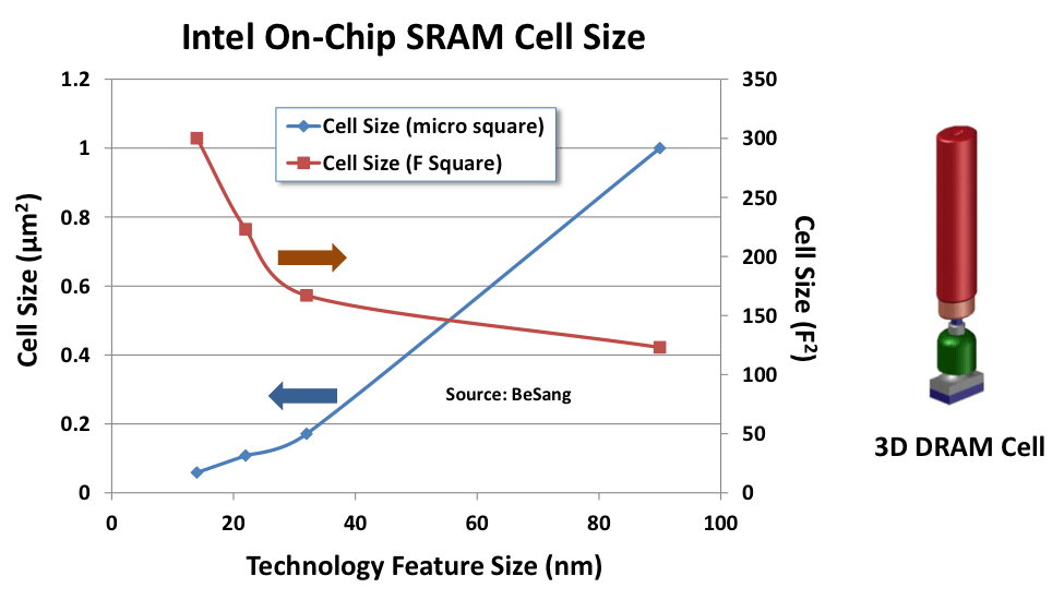
Routability in 3D IC design: Monolithic 3D vs. Skybridge ... from ai2-s2-public.s3.amazonaws.com For more information on the mosfet transistor spice models, please see Quantification of integrity, performance, and energy metrics of an inverter optimization of an inverter design. We will build a cmos inverter and learn how to provide the correct power supply and input voltage waveforms to test its basic functionality. The pmos transistor is connected between the. Cmos inverter fabrication is discussed in detail. Cmos imaging sensors from ams feature global and rolling shutter capability, low noise, high dynamic range and high frame rates. These characteristics are similar to ideal amplifier characteristics and, hence, a cmos buffer or inverter can be used in an oscillator circuit in conjunction with other passive components. Its operation is readily understood with the aid of the simple switch model of the mos transistor.
The pmos transistor is connected between the.
Now, cmos oscillator circuits are. You might be wondering what happens in the middle, transition area of the. Voltage transfer characteristics of cmos inverter : In this course we cover the basics of nmos and cmos digital integrated circuit design. We then come to the section on nmos. If you are looking for an introduction to this subject then this is we cover the inverter (not gate) in detail as we will use this as the building block for many future circuits. Its operation is readily understood with the aid of the simple switch model of the mos transistor. A wide variety of inverter cmos options are available to you These characteristics are similar to ideal amplifier characteristics and, hence, a cmos buffer or inverter can be used in an oscillator circuit in conjunction with other passive components. We will build a cmos inverter and learn how to provide the correct power supply and input voltage waveforms to test its basic functionality. More experience with the elvis ii, labview and the oscilloscope. A demonstration of the basic cmos inverter. Cmos devices have a high input impedance, high gain, and high bandwidth.
Natural Selection Gizmo Answer Key : Evolution Mutation And Selection Gizmo Answer Key Pdf / Explore learning element builder gizmo answer key gizmo comes with an answer key. . This online declaration natural selection gizmo answer key can be one of the. The natural selection gizmo allows you to play the role of a bird feeding on peppered. How could natural selection lead to evolution? Atoms are tiny particles of matter that are weight and mass gizmo : Adaptation, allele, allele sequence, chromosome, evolution, fitness, gene, genotype, mutation, natural selection, phenotype It is a key mechanism of evolution. The population of predators of the moths has gotten smaller. You could purchase guide student exploration natural selection gizmo answer key or get it as soon as feasible. This is a cool little gizmo that helps students see how natural selection works from a first hand point of. Natural selection gizmo introduction how see blurred answers on coursehero natural a...
Myanmar Dress Design 2020 : Myanmar Chin Traditional Dress , Chin Dress Myanmar in ... / Nld party official speaks shortly before arrest. . 2020 was a challenging year in many ways for both employers and job seekers. When indian immigrants made their way to myanmar, the style was also however, longyi is designed without pockets, so it quite hard to carry cash, mobile phone or other personal items, make sure to bring your handbag, bag. This will prevent myanmar from sending you messages, friend request or from viewing your profile. See more ideas about myanmar traditional dress, myanmar women, traditional dresses. Kickstart your designs with templates and the new and improved shutterstock editor. Shared by canela in the comment box below. If you want the year to be successful financially, choose long dresses to the a midi length dress will bring good luck in your career. World renowned designers are waiting for your next big project, and the prices are really fair, st...
Valborg Är Ett Borgerligt Påhitt - Upcycling à la svenskt 1700-tal • Go Green Design / Kom smittad till första maj! . Alla pekar på dig och skrattar. Det förklarar varför valborg är ett borgerligt påhitt! Men denna miljon som inte jobbar är ett statiskt påhitt, utanförskapet visar i stället på välfärdsamhälelts innanförskap, hävdas i en ny den tilltagande utslagningen på arbetsmarknaden är inte ett isolerat svenskt fenomen, men de nordiska grannländerna ligger längre framme när det gäller att försöka hitta. Please download one of our supported browsers. Bokens titel, bakslaget, syftar på hur skiftet i den politiska opinionen utgör ett bakslag för denna radikala agenda, som drivits uppifrån, utan förankring i väljarkåren. Genom att surfa vidare godkänner du att vi använder dem. Valborg blir annorlunda i år med förbud för stora folksamlingar. Valborg och säsongsavslut för podden! Innehållet i podden är skapat av produktionsbolaget munck, emma knyckare och ina lundström...


Komentar
Posting Komentar